


Cookies help us deliver our services. By using our services, you agree to our use of cookies.
- Register
- Log in
-
Shopping cart
(0)
You have no items in your shopping cart.
Search
FIRST Componens Academy | MIPI DSI Compatibility and Timing in Display Integration
Friday, March 20, 2026
From Winstar News of March '26
MIPI DSI Compatibility and Timing Mechanisms in Display System Integration
In display product development and system integration, it is not uncommon to encounter initialization failure or unstable display behavior—even when both the host SoC and the display driver IC (DDIC) are specified as MIPI DSI compliant.
Typical symptoms include black screens, intermittent vertical noise lines, or inconsistent display stability across different hardware platforms. These issues are often attributed to panel hardware or initialization sequences. However, practical integration experience shows that the root cause is frequently related to D-PHY timing margin during LP-to-HS transition, rather than protocol-level incompatibility.
If physical layer behavior and system boundary conditions are not evaluated during early design stages, integration risks may still occur—even when the panel fully complies with the MIPI specification.
MIPI DSI Architecture and Layer Interaction
MIPI DSI consists of two major layers:
Physical Layer (D-PHY / C-PHY)
Responsible for:
• Electrical signal transmission
• Lane state transitions
• High-speed data transfer
• Timing window control
Protocol Layer
Responsible for:
• Packet structure definition
• Header format
• ECC/CRC protection
• Command mode and video mode data organization
In practical system integration, if physical layer timing does not fall within the receiver’s acceptable detection window, packet synchronization and header parsing may fail—triggering protocol-level error handling mechanisms.
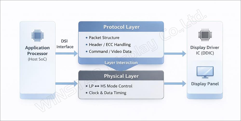
【Figure 1】 MIPI DSI system-level architecture and layer interaction
D-PHY Transmission Mechanism and Timing Sensitivity
MIPI DSI uses DDR (Double Data Rate) transmission, sampling data on both rising and falling clock edges.
• The duration of one bit is defined as the Unit Interval (UI)
• One DDR cycle equals 2 × UI
As D-PHY data rate increases, system sensitivity also increases in the following areas:
• PLL jitter
• LP-to-HS transition timing
• Receiver startup delay
• Signal integrity
While higher data rates improve display performance, they also reduce allowable timing margin.
LP-to-HS Transition and Timing Requirements
Before entering High-Speed (HS) mode, the transmitter must complete the LP-to-HS transition:
• LP-11 (Idle)
• LP-01 → LP-00
• THS-PREPARE
• THS-ZERO
• SoT (Start of Transmission)
According to the D-PHY v1.1 specification: THS-PREPARE + THS-ZERO > 145 ns + 10 × UI
However, in real-world display system integration, meeting the minimum specification limit may not guarantee cross-platform stability. In practical engineering design, additional timing margin is typically required to reduce integration risk.
![]()
【Figure 2】MIPI D-PHY LP-to-HS mode transition timing diagram
Practical Observation: HS-Settle Requirements Beyond Theoretical Minimum
During cross-platform MIPI DSI bring-up testing, it has been observed that in certain ARM-based SoC platforms paired with DSI v1.1 DDIC devices, stable display operation required: THS-PREPARE + THS-ZERO > 215 ns
This behavior is related to receiver-side design characteristics:
• HS receiver requires stabilization time before sampling
• Internal filtering mechanisms introduce detection delay
• If SoT transmission occurs too early, receiver startup may be incomplete
When SoT detection fails:
• Byte alignment failure
• Header parsing errors
• ECC mismatch
• Packet discard
At system level, these errors typically manifest as black screens or unstable display output.
SoT Detection and Packet Integrity
SoT (Start of Transmission) is the synchronization sequence marking the beginning of high-speed data.
The receiver must successfully:
• Enter HS mode
• Lock timing
• Perform bit-level sampling within the correct timing window
If SoT detection fails, the following issues may occur:
• Byte alignment errors
• Header decode failure
• ECC verification errors
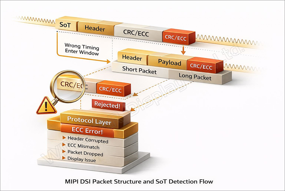
【Figure 3】MIPI DSI packet structure and SoT detection flow
DSI Version Compatibility and Platform Differences
Matching DSI version numbers only indicates specification-level compatibility. It does not guarantee identical implementation behavior.
Different SoC platforms may vary in:
• PLL architecture
• Adjustable transition timing parameters
• Receiver HS-Settle detection mechanisms
• PHY tuning configuration methods
Some platforms provide limited adjustment ranges for D-PHY timing parameters, which may constrain integration flexibility.
Therefore, display system integration should evaluate actual platform implementation characteristics and tuning capability, rather than relying solely on version compliance.
Engineering Considerations in Display System Integration
MIPI DSI compatibility is influenced by multiple system-level factors:
• SoC PHY architecture and jitter characteristics
• PCB impedance control and signal integrity
• Power stability
• EMI and environmental noise conditions
• Bridge IC or adapter circuitry
WINSTAR Practical Experience in MIPI DSI Integration
Through cross-platform MIPI DSI bring-up and compatibility validation projects, WINSTAR has observed that physical layer timing margin and receiver detection behavior significantly impact overall system stability.
During display integration projects, WINSTAR includes the following validation steps:
• LP-to-HS transition margin analysis
• SoT detection stability testing
• Multi-platform cross verification
• PCB signal integrity evaluation
• Module-to-platform compatibility assessment
Conclusion
MIPI DSI is a high-performance display interface. However, real-world compatibility is not determined solely by specification compliance.
Engineering practice shows:
• Specification minimum values represent baseline requirements; additional timing margin is often necessary for stable system integration.
• PHY and Protocol layers must be evaluated together.
• Platform implementation differences may affect SoT detection and data locking behavior.
• Display system integration requires cross-layer timing and packet stability validation.
Evaluating LP-to-HS transition margin and receiver startup behavior early in product development can significantly reduce late-stage integration risks.
FAQ – MIPI DSI Integration and Timing
Q1: Why can a black screen occur even when DSI specification is met?
Even if the specification is met, insufficient LP-to-HS timing margin may cause SoT detection failure, leading to packet discard and no display output.
Q2: Does matching DSI version guarantee compatibility?
No. Differences in PHY and receiver implementation across platforms can impact real-world compatibility.
Q3: Is meeting the HS-Settle minimum specification sufficient?
In practical cross-platform integration, additional timing margin is often required for stable operation.
Q4: Why is cross-layer validation necessary in display integration?
Because DSI compatibility is influenced by both physical and protocol layers, system-level validation is required to ensure stable performance.