DRAWING
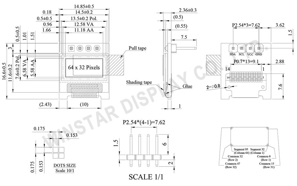
SPECIFICATIONS
Interface Pin Function
| No. | Symbol | Function |
|---|
| 1 |
GND |
Ground |
| 2 |
VCC |
Power supply input. |
| 3 |
SCL |
When the I2C interface is selected, then D0 serves as the serial clock input pad (SCL) and D1 serves as the serial data input pad (SDAI). |
| 4 |
SDA |
Mechanical Data
| Item | Dimension | Unit |
|---|
| Dot Matrix |
64 x 32 |
Dots |
| Module dimension |
14.85 × 16.6 × 2.36 |
mm |
| Active Area |
11.18 × 5.58 |
mm |
| Pixel Size |
0.153 × 0.153 |
mm |
| Pixel Pitch |
0.175 × 0.175 |
mm |
| Display Mode |
Passive Matrix |
| Display Color |
Monochrome |
| Drive Duty |
1/32 Duty |
| IC |
SSD1306 |
| Interface |
I2C |
| Size |
0.49 inch |
Absolute Maximum Ratings
| Parameter | Symbol | Min | Max | Unit |
|---|
| Supply Voltage for Logic |
VCC |
0 |
4.0 |
V |
| Supply Voltage for Display |
VCC1 |
0 |
16.0 |
V |
| Operating Temperature |
TOP |
-40 |
+80 |
°C |
| Storage Temperature |
TSTG |
-40 |
+85 |
°C |
Electronical Characteristics
| Item | Symbol | Condition | Min | Typ | Max | Unit |
|---|
| Supply Voltage for Logic |
VCC |
- |
2.8 |
3.0 |
3.2 |
V |
| Input High Volt. |
VIH |
- |
0.8×VDD |
- |
VDDIO |
V |
| Input Low Volt. |
VIL |
- |
0 |
- |
0.2×VDD |
V |
| Output High Volt. |
VOH |
- |
0.9×VDD |
- |
VDDIO |
V |
| Output Low Volt. |
VOL |
- |
0 |
- |
0.1×VDD |
V |
| 50% check Board operating Current |
ICC |
VCC1=7.5V |
- |
13.0 |
26.0 |
mA |
Specifiche di prodotto
|
Size
|
0.49" |
|
Resolution
|
64x32 |
|
Active Area (mm)
|
11.18x5.58 |
|
Dot Size
|
0.15x0.15 |
|
Polarizer
|
Glare |
|
Color
|
Yellow |
|
Power supply
|
3V |
|
Display Interface
|
I2C |
|
Display IC
|
SSD1306BZ |
|
Constructive Structure
|
COG + PCB |
|
Frame
|
No |
|
Touch Panel
|
No touch |
|
O. Temperature (°C)
|
-40~80 |
|
Data Connection
|
Pin Strip |
|
Pin Nr.
|
4 |
|
Pin Pitch
|
2.54mm |
|
Preferred - Not Preferred
|
Not Preferred |