DESCRIPTION
WAA0213BA6#A2N1AA-FC is an Electronic Paper Display (EPD) with a front light panel. The display is capable of showing images in 1-bit black and white with full display capabilities. The 2.13-inch active area has a resolution of 122 × 250 pixels. The module is a TFT-array-driven electrophoretic display with integrated circuits, including a gate driver, source driver, MCU interface, timing controller, oscillator, DC-DC converter, SRAM, LUT, and VCOM. This module can be used in portable electronic devices, such as Electronic Shelf Label (ESL) systems.
Features
- 122×250 pixels display
- High contrast, high reflectance
- Ultra wide viewing angle
- Ultra low power consumption
- Pure reflective mode
- Bi-stable display
- Commercial temperature range
- Landscape and portrait modes
- Hard-coat, antiglare display surface
- Ultra low current deep sleep mode
- On-chip display RAM
- Waveforms can be stored in the on-chip OTP or written by the MCU
- Serial peripheral interface available
- On-chip oscillator
- On-chip booster and regulator control for generating VCOM, Gate, and Source driving voltages
- I2C master interface to read external temperature sensor. Built-in temperature sensor
- With front light panel, 3 LEDs in serial
- Operating voltage for front light panel: 9V
DRAWING
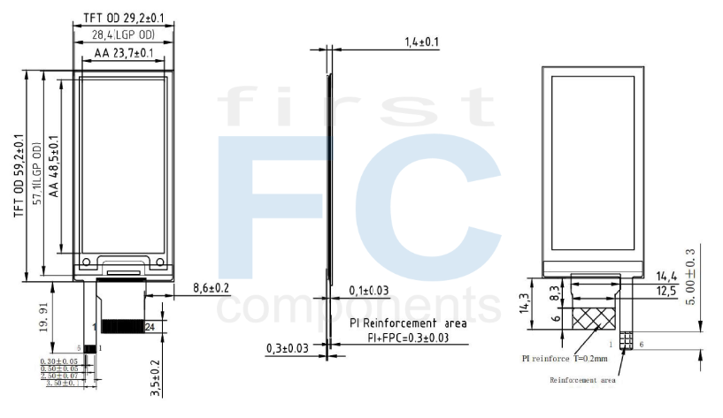
SPECIFICATIONS
General Specifications
| Parameter | Specifications | Unit |
|---|
| Screen Size |
2.13 |
Inch |
| Display Resolution |
122(H)×250(V) |
Pixel |
| Active Area |
23.7×48.5 |
mm |
| Pixel Pitch |
0.1943×0.1942 |
mm |
| Pixel Configuration |
Square |
|
| Outline Dimension |
29.2(H)×59.2 (V) ×1.4(D) |
mm |
| Module Weight |
4.75±0.5 |
g |
Electrical Characteristics
Absolute Maximum Ratings
| Parameter | Symbol | Rating | Unit |
|---|
| Logic supply voltage |
VCI |
-0.5 to +4.0 |
V |
| Logic Input voltage |
VIN |
-0.5 to VCI +0.5 |
V |
| Logic Output voltage |
VOUT |
-0.5 to VCI +0.5 |
V |
| Operating Temp range |
TOPR |
0 to +50 |
ºC |
| Storage Temp range |
TSTG |
-25 to+70 |
ºC |
| Optimal Storage Humidity |
HSTGo |
55±10 |
%RH |
Interface
Input /Output Pin Assignment
| No. | Name | I/O | Description |
|---|
| 1 |
NC |
|
Do not connect with other NC pins |
| 2 |
GDR |
O |
N-Channel MOSFET Gate Drive Control |
| 3 |
RESE |
I |
Current Sense Input for the Control Loop |
| 4 |
NC |
NC |
Do not connect with other NC pins |
| 5 |
VSH2 |
C |
Positive Source driving voltage(Red) |
| 6 |
TSCL |
O |
I2C Interface to digital temperature sensor Clock pin |
| 7 |
TSDA |
I/O |
I2C Interface to digital temperature sensor Data pin |
| 8 |
BS1 |
I |
Bus Interface selection pin |
| 9 |
BUSY |
O |
Busy state output pin |
| 10 |
RES# |
I |
Reset signal input. Active Low. |
| 11 |
D/C# |
I |
Data /Command control pin |
| 12 |
CS# |
I |
Chip select input pin |
| 13 |
SCL |
I |
Serial Clock pin (SPI) |
| 14 |
SDA |
I/O |
Serial Data pin (SPI) |
| 15 |
VDDIO |
P |
Power Supply for interface logic pins It should be
connected with VCI |
| 16 |
VCI |
P |
Power Supply for the chip |
| 17 |
VSS |
P |
Ground |
| 18 |
VDD |
C |
Core logic power pin VDD can be regulated internally from VCI. A capacitor should be connected between VDD and VSS |
| 19 |
VPP |
P |
FOR TEST |
| 20 |
VSH1 |
C |
Positive Source driving voltage |
| 21 |
VGH |
C |
Power Supply pin for Positive Gate driving voltage
and VSH1 |
| 22 |
VSL |
C |
Negative Source driving voltage |
| 23 |
VGL |
C |
Power Supply pin for Negative Gate driving voltage
VCOM and VSL |
| 24 |
VCOM |
C |
VCOM driving voltage |
Specifiche di prodotto
|
Size
|
2.13" |
|
Resolution
|
250x122 |
|
Active Area (mm)
|
23.71x48.55 |
|
Dot Size
|
0.19x0.19 |
|
Color
|
Black on White |
|
Display Interface
|
SPI |
|
O. Temperature (°C)
|
0~50 |
|
Data Connection
|
FPC for ZIF Connector |
|
Pin Nr.
|
24 |
|
Pin Pitch
|
0.5mm |
|
Preferred - Not Preferred
|
Preferred |