DESCRIPTION
The round OLED CTP +Knob model is an extension item which equipped with capacitive touch screen and a control knob on module, it's an Ø1.18" circular COG type OLED display; made of resolution 128x128 dots. This OLED Touch Encoder module is built in with SSD1327 IC, it supports 4-line SPI and I2C interface, supply voltage for logic 3V (typical value), 1/128 driving duty. This model is built in with FT3268 touch panel IC on module, which supports I2C interface, one detect point for capacitive touch screen.
This round OLED with capacitive touch screen and Knob is ideal for applications which required a control knob on devices such as smart home applications, intelligent technology devices, audio system, etc. This module can be operating at temperatures from -20℃ to +50℃; its storage temperatures range from -30℃ to +70℃.
DRAWING
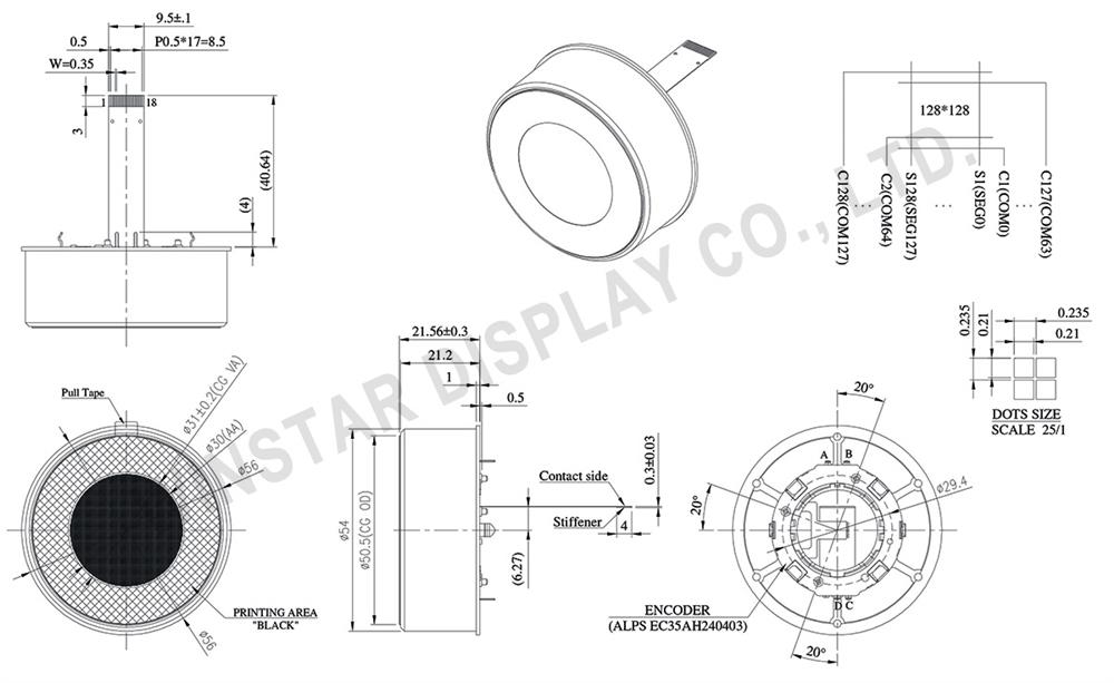
SPECIFICATIONS
Interface Pin Function
| No. | Symbol | Function |
|---|
| 1 |
VSS |
Ground pin. It must be connected to external ground. |
| 2 |
VCC |
Power supply for panel driving voltage. This is also the most positive power voltage supply pin. It is supplied by external high voltage source. |
| 3 |
VCOMH |
COM signal deselected voltage level. A capacitor should be connected between this pin and VSS. No external power supply is allowed to connect to this pin. |
| 4 |
VCI |
Low voltage power supply and power supply for interface logic level. It should match with the MCU interface voltage level and must be connected to external source. VCI must always set to be equivalent to or higher than VDD. |
| 5 |
VDD |
Power supply pin for core logic operation.
VDD can be supplied externally (within the range of 2.4V to 2.6V) or regulated Internally from VCI. A capacitor should be connected between VDD and VSS under all circumstances. |
| 6 |
BS1 |
MCU bus interface selection pins. Select appropriate logic setting as described in the following table. BS1 is pin select. Bus Interface selection
| BS1 | Interface |
|---|
| 0 |
4-line SPI |
| 1 |
I2C |
Note (1) 0 is connected to VSS (2) 1 is connected to VCI |
| 7 |
IREF |
This pin is the segment output current reference pin |
| 8 |
CS# |
This pin is the chip select input connecting to the MCU. The chip is enabled for MCU communication only when CS# is pulled LOW (active LOW). |
| 9 |
RES# |
This pin is reset signal input. When the pin is pulled LOW, initialization of the chip is executed. Keep this pin pull HIGH during normal operation. |
| 10 |
DC# |
This pin is Data/Command control pin connecting to the MCU. When the pin is pulled HIGH, will be interpreted as data. When the pin is pulled LOW, will be transferred to a command register In I2C mode, this pin acts as SA0 for slave address selection. |
| 11 |
D0 |
When serial interface mode is selected, D0 will be the serial clock input: SCLK; D1 will be the serial data input: SDIN and D2 should be kept NC. When I2C mode is selected, D2, D1 should be tied together and serve as SDAout , SDAin in application and D0 is the serial clock input, SCL. |
| 12 |
D1 |
| 13 |
D2 |
| 14 |
TP_SCK |
I2C clock signal |
| 15 |
TP_SDA |
I2C data signal |
| 16 |
TP_INT |
Interrupt signal |
| 17 |
VCC |
Power supply for panel driving voltage. This is also the most positive power voltage supply pin. |
| 18 |
VSS |
Ground |
Encoder PIN Definition
| No. | Symbol | Function |
|---|
| 1 |
FSW_A |
Encoder terminal signal-A |
| 2 |
FSW_B |
Encoder terminal signal-B |
| 3 |
FSW_C |
Encoder terminal signal-C |
| 4 |
FSW_D |
Ground |
Mechanical Data
| Item | Dimension | Unit |
|---|
| Dot Matrix |
128 × 128 |
Dots |
| Module dimension |
Ø56 × 21.56 |
mm |
| Active Area |
Ø30.0 |
mm |
| Pixel Size |
0.210 × 0.210 |
mm |
| Pixel Pitch |
0.235 × 0.235 |
mm |
| Display Mode |
Passive Matrix |
| Display Color |
Monochrome |
| Drive Duty |
1/128 Duty |
| Gray Scale |
4 bits |
| IC |
SSD1327 |
| Interface |
4-line SPI , I2C |
| Size |
1.18 inch |
| CTP IC |
FT3268 |
| Detect Point |
1 |
| CTP Interface |
I2C |
Absolute Maximum Ratings
| Parameter | Symbol | Min | Max | Unit |
|---|
| Supply Voltage for Operation |
VCI |
-0.3 |
4.0 |
V |
| Supply Voltage for Logic |
VDD |
-0.5 |
2.75 |
V |
| Supply Voltage for Display |
VCC |
-0.5 |
19.0 |
V |
| Operating Temperature |
TOP |
-20 |
+70 |
°C |
| Storage Temperature |
TSTG |
-30 |
+70 |
°C |
Electronical Characteristics
DC Electrical Characteristics
| Item | Symbol | Condition | Min | Typ | Max | Unit |
|---|
| Supply Voltage for Operation |
VCI |
- |
2.8 |
3.0 |
3.3 |
V |
| Supply Voltage for Display |
VCC |
- |
8.0 |
14.5 |
15.0 |
V |
| Supply Voltage for Logic |
VDD |
- |
1.65 |
- |
2.6 |
V |
| High Level Input |
VIH |
- |
0.8×VCI |
- |
VCI |
V |
| Low Level Input |
VIL |
- |
0 |
- |
0.2×VCI |
V |
| High Level Output |
VOH |
Iout = 100uA |
0.9×VCI |
- |
VCI |
V |
| Low Level Output |
VOL |
Iout = 100uA |
0 |
- |
0.1×VCI |
V |
| 50% Check Board operating Current |
VCC =14.5V |
- |
15 |
30 |
mA |
Touch Panel Controller FT3268
| Item | Symbol | Condition | Min | Typ | Max | Unit |
|---|
| Input High Volt. |
VIH |
- |
0.7×VDD |
- |
VDD |
V |
| Input Low Volt. |
VIL |
- |
-0.3 |
- |
0.3×VDD |
V |
| Output High Volt. |
VOH |
IOH = 0.1mA |
0.7×VDD |
- |
- |
V |
| Output Low Volt. |
VOL |
IOL = 0.1mA |
- |
- |
0.3×VDD |
V |
Specifiche di prodotto
|
Size
|
1.18" |
|
Resolution
|
128x128 |
|
Active Area (mm)
|
Ø30.00 |
|
Dot Size
|
0.21x0.21 |
|
Polarizer
|
Glare |
|
Color
|
White |
|
Power supply
|
3V |
|
Display Interface
|
SPI/I2C |
|
Display IC
|
SSD1327 |
|
Constructive Structure
|
Circular Knob COG |
|
Frame
|
No |
|
Touch Panel
|
Capacitive |
|
O. Temperature (°C)
|
-20~50 |
|
Data Connection
|
FPC for ZIF Connector |
|
Pin Nr.
|
18 |
|
Pin Pitch
|
0.5mm |
|
Touch Panel IC Controller
|
FT3268 |
|
Preferred - Not Preferred
|
Not Preferred |